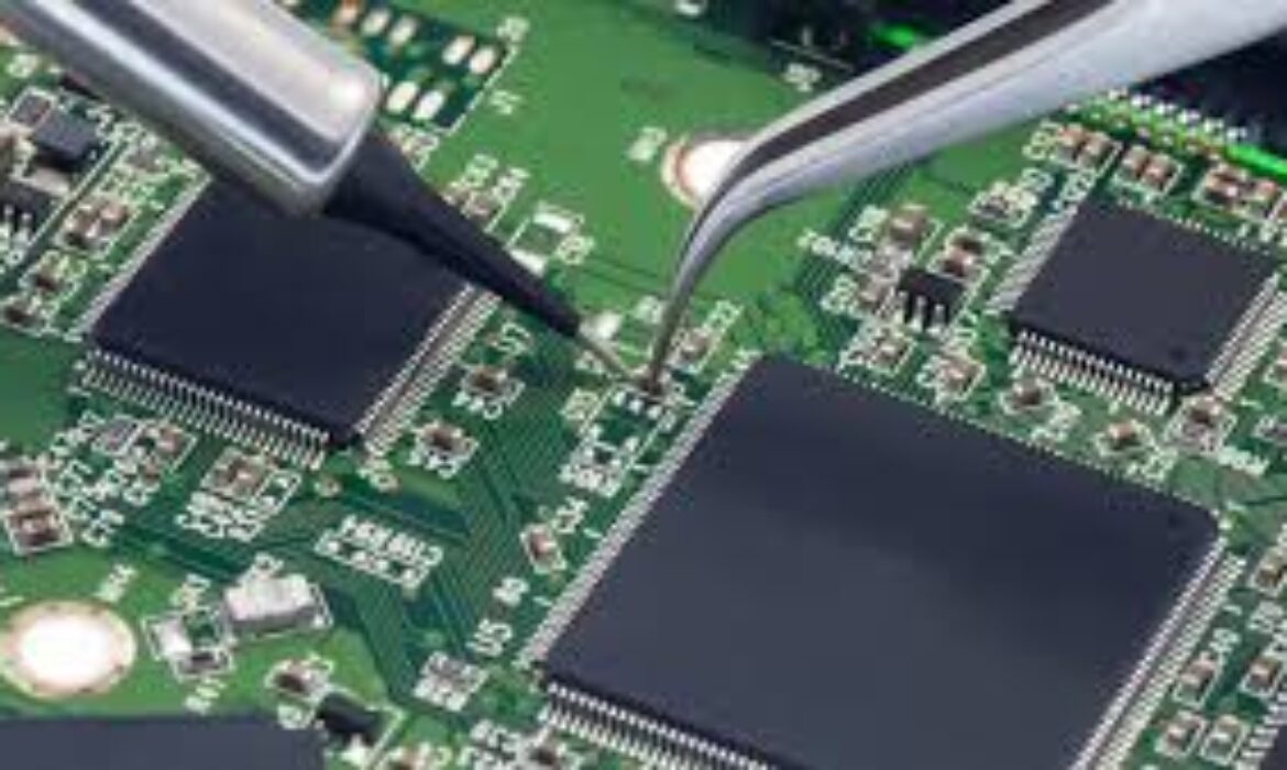
The PCBA process is now central to modern electronics manufacturing. This is a complex process. Engineers build and link systems with circuits in a printed circuit board, or PCB. This forms a working electronic system. It is crucial to examine each step of the PCBA process and its control points. This enables us to control the outcome and be effective. This guide will detail each step. It will cover key control points to install throughout the process. For more details on factors that affect PCB Assembly costs, see our article on PCB assembly costs.
Design and Prototyping:
The first, and a key, step in PCBA manufacturing is to design and develop prototypes. This stage starts with a design for creation. It makes detailed PCB designs using electronic design automation software.
Engineers prepare conceptual electrical interconnection maps. These describe the interconnections between each part. They also create a PCB layout.
Precise definitions and strategic placements of a circuit’s elements are crucial. This will improve the circuit’s specifications and reliability.
Creating a printed circuit board layout from the design files involves prototyping. Someone created the layout in a virtual environment. This step is also important. It helps find design defects that may go unnoticed in the production of the whole units.
PCB Fabrication:
The second important process of PCBA manufacturing after prototyping is fabrication. It checks the design’s feasibility. At this stage, we make the printed circuit board from raw materials. The design shapes it according to the circuit board’s development.
Fabrication includes choosing, modifying, and processing the materials. The primary material is the PCB substrate. It consists of epoxy resin reinforced with fiberglass. PCBs may consist of ceramic or flexible materials for specific applications. It forms the base of the board and also offers electrical isolation to the board.
- Material Selection: The PCB’s substrate and copper layers are high quality. They are handpicked.
- Fabrication Process: It includes lamination, drilling, etching, and solder masks. These steps make the final PCB.
Key Control Points:
- Material Quality: Use high-quality materials to make the PCB. This will improve its durability and performance.
- Precision in Fabrication: Drilling and etching must be accurate. Flaws from these processes could hinder assembly.
Sourcing:
Component sourcing is the process of acquiring the parts to assemble the PCB. They are electronic parts. Based on the design process, we do this. It focuses on finding reliable suppliers. Their components must meet the required quality and performance. This is crucial for product reliability. Also important is inventory management. It answers how much stock to hold to avoid production line disruptions.
Building a good relationship with the supplier is key. It will help us keep the right inventory for production needs. This will prevent long interruptions and delays in component delivery. It will keep the assembly line effective and productive.
Key Control Points:
- Component Quality: Assure the quality and genuineness of all parts.
- Timely Procurement: Make sure that parts are on hand then so that an assembly line is not held up.
Component Placement:
Component placement is the last stage of PCBA construction. It involves placing electronic components on the PCB. Hand or customized equipment positions items. Workers position individual components in sequence. Small runs of printed circuit boards or prototypes use them.
This method places many components at once. But automated placement machines are the most used method for high production rates.
These machines boast cutting-edge technology. They install many components with accuracy and speed. Automated placement is efficient on the production line. It also ensures that all assembled PCBs are of high quality.
Key Control Points:
- Components must have precise placement to prevent misalignment and ease of connection.
- Inspection: Install checks to identify placement errors before soldering.
Soldering:
Soldering is one of the most sensitive processes in PCBA production. It uses solder to connect individual electronic components to the PCB. This provides reliable electrical connections. There are several ways to solder. The batch size and the pieces to be soldered determine it. The elements can be small or large. For through-hole components.
Wave soldering is the most used method. A wave of solder passes through the final, built PCB. This fixes the component leads to the board pads.
Reflow soldering is also applied in assembly applications and surface mount components. This is a technique. First, we deposit solder paste on the PCB. Then, we place the components in their positions. The components are then placed where needed on the PCB and the board. The heat from the reflow oven solders them together.
We choose each part based on its suitability for the array output in a given cycle. This ensures the best soldering quality and speed.
Inspection and Testing:
After soldering, we check the PCB. This confirms that all components are secure and functioning. The technicians will use their naked eyes to search the board for signs of a problem.
To increase process speed and reliability, we use AOI systems. They find defects that the naked eye cannot, like disposals or short circuits. X-ray inspection shows the inner connections of hidden solder joints. It ensures that the soldering work is correct.
After inspecting, the team conducts a functional test. The goal is to verify the PCB’s correct operation across modes. This testing simulates the field environment. It checks whether the board works as intended.
The inspection and testing procedures aim to ensure quality. They must confirm the PCB works in its intended applications and reduce failures.
Rework and Repair:
If inspection or testing finds defects, we must fix them to meet quality standards. Rework techniques solved various issues. They swapped out flawed solder joints and malfunctioning parts instead.
This procedure takes a lot of work. It needs a careful disconnection of faulty parts and replacing them with good ones. We also fix issues like solder bridges or bad splashes. We do this by reapplying or modifying the solder to make a strong connection.
The rework can restore the PCB to its intended function. It can then pass inspection and testing and get approval.
Final Assembly and Packaging:
The last step in PCB manufacturing is to accept the board into its final housing and packaging. This phase starts by placing and mounting the PCB in a case. Then, add any parts or ports needed for the PCB’s functionality. Finally, we accommodate the board to protect it during transport.
Key control considerations at this stage are to ensure the assembly is secure. Also, connections must be tight and rigid. Good packaging prevents damage and protects the PCB from static in transit. If you want to use professional and trusted services, please visit at kingsunpcba.com
Conclusion:
It is important to know and control the main stages and key points of PCB manufacturing. Each stage of development, from design to assembly, has critical tasks. They must precise execution to guarantee the product’s dependability and functionality. For tips on getting the best value in your PCBA manufacturing, visit our website.


